

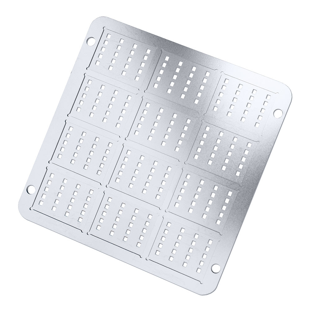
The Ossila E339 High Density Active Area Deposition Mask is a stainless steel evaporation mask that defines the active area of devices built with Ossila's high-density OFET system. Each substrate carries 20 OFETs, and the E339 version holds 12 substrates (S233, S411).
Two configurations are offered. The direct contact version, with no spacer, suits sputtering and other non-directional deposition methods, and also thermal deposition at oblique angles or with a very short throw, where it gives well-defined edges. The version with a 100 μm spacer is suited to standard thermal evaporation, helping to prevent scratches and improving out-gassing.
The mask measures 75 mm x 75 mm (2.95" x 2.95"), with a thickness of 1.7mm without spacer or 1.8mm with spacer (exc. bolts). Linear channel and interdigitated channel variants are available. For interdigitated FETs, the source-drain, active area and gate masks must all be swapped for their matching versions.
- Depositing the active layer of OFETs in Ossila's high-density FET system.
- Sputtering and other non-directional deposition using the direct contact mask.
- Standard thermal evaporation using the mask with 100 μm spacer.
- Fabricating back-gate FETs on Si/SiO2 or other substrates, and front-gate FETs on any substrate, together with the other system masks.
| Brand | Ossila |
|---|---|
| CAS number | — |
| Molecular formula | — |
| Purity | — |
| Category | — |
| Pack sizes | — |
| Physical form | — |
| Storage | — |
- Product code: E339
- Product code: E339
- Size: 75 mm x 75 mm (2.95" x 2.95")
- Thickness: 1.7mm without spacer, 1.8mm with spacer (exc. bolts)
- Material: Stainless steel
- Substrate capacity: 12 (S233, S411)
- Number of OFETs: 20 per substrate
- Spacer option: No spacer (direct contact) or 100 μm spacer
—
—