

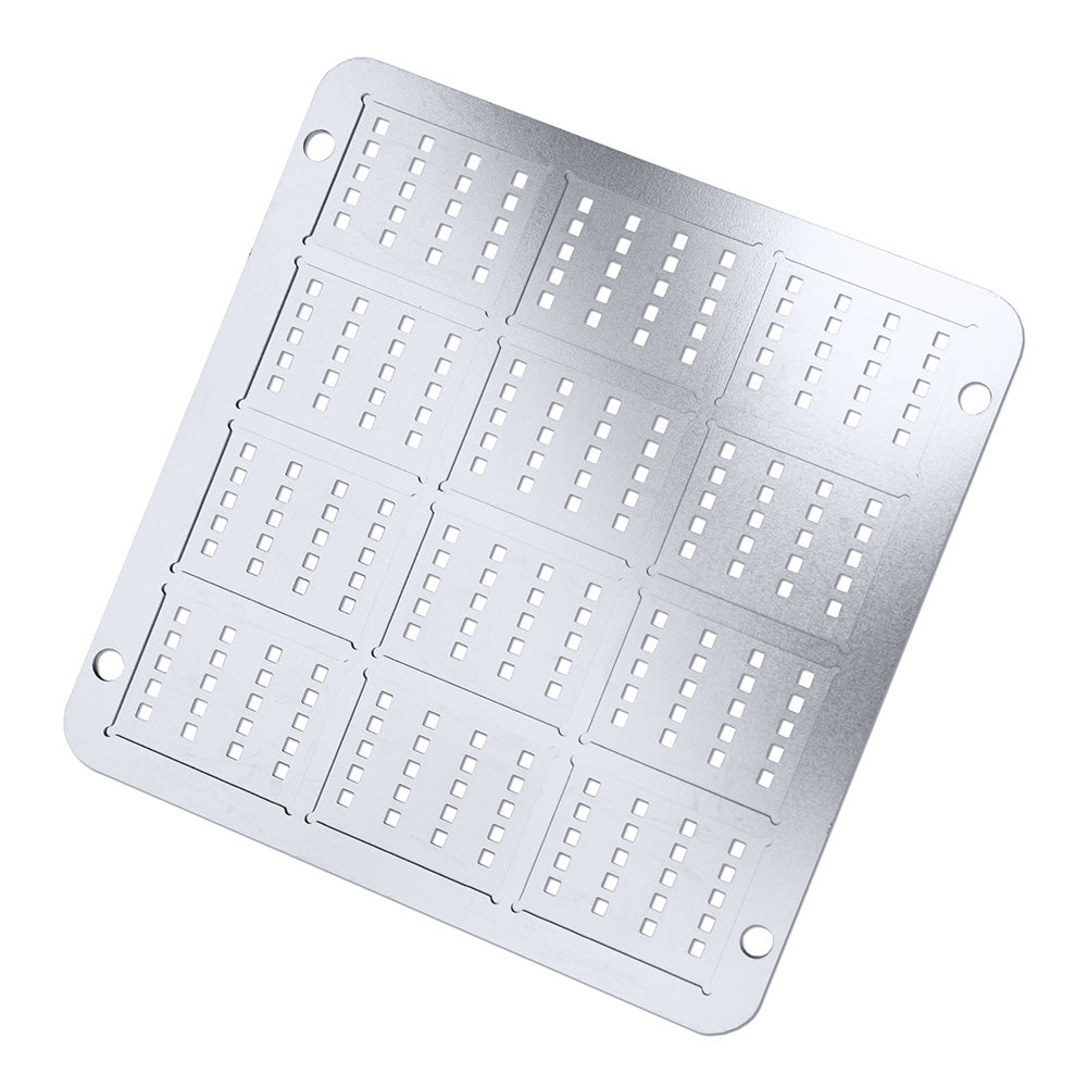
The Ossila High Density Active Area Deposition Mask is a stainless steel evaporation mask used to pattern the active area of transistor devices. It is designed to work as part of Ossila's high-density OFET system, where each substrate carries 20 OFETs.
The mask is offered in versions for linear channel and interdigitated channel high-density OFETs, each with or without a spacer layer. The direct contact version (no spacer) is suited to sputtering and other non-directional deposition methods, and to thermal deposition setups with oblique angles or a very short throw, where it helps produce sharply defined edges. The version with a 100 μm spacer is intended for standard thermal evaporation, reducing the risk of scratching the substrate and improving out-gassing.
The mask measures 75 mm x 75 mm and is 1.7mm thick without spacer or 1.8mm with spacer (excluding bolts). When building interdigitated FETs, the source-drain, active area and gate masks should all be the matching interdigitated versions.
- Depositing the active layer of OFETs fabricated with Ossila's high-density OFET system.
- Patterning active areas by thermal evaporation using the 100 μm spacer version.
- Active area deposition by sputtering or other non-directional methods using the direct contact version.
- Fabricating back-gate FETs on Si/SiO2 or other substrates, and front-gate FETs on any substrate, together with the matching system masks.
| Brand | Ossila |
|---|---|
| CAS number | — |
| Molecular formula | — |
| Purity | — |
| Category | — |
| Pack sizes | — |
| Physical form | — |
| Storage | — |
- Product code: E339-SPC
- Number of OFETs: 20 per substrate
- Size: 75 mm x 75 mm (2.95" x 2.95")
- Thickness: 1.7mm without spacer, 1.8mm with spacer (exc. bolts)
- Material: Stainless steel
- Spacer: 100 μm
- Substrate capacity (E339): 12 (S233, S411)
—
—