

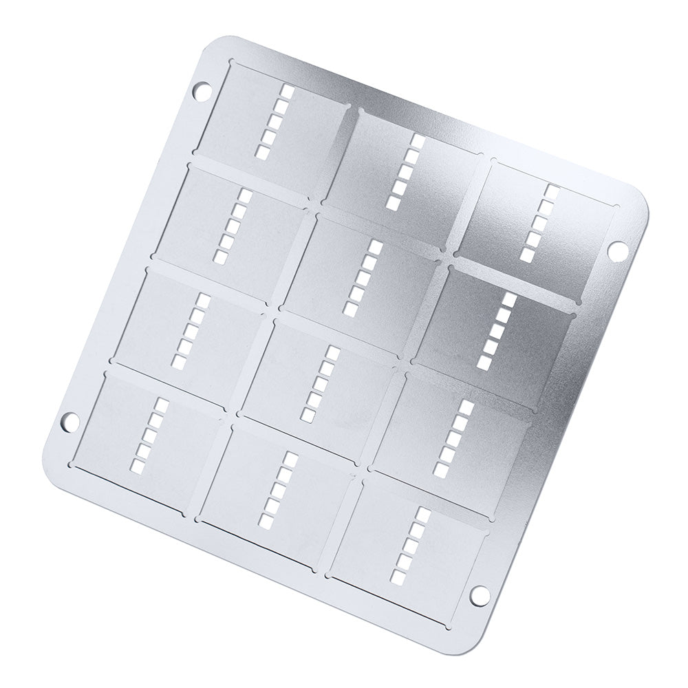
This Ossila mask is used to evaporate material into the active area of a transistor, meaning the source-drain channels. It belongs to the low density OFET fabrication system and is intended for use alongside the other masks in that set on 20 mm x 15 mm substrates.
Two variants are offered. The version with a 100 μm standoff spacer keeps the mask clear of the substrate while still giving good deposition resolution; it suits standard thermal evaporation, helping to prevent scratches and improving out-gassing. The direct contact version is the better choice for sputtering and other non-directional methods, or for thermal deposition at oblique angles or with a very short throw, where it gives sharply defined edges.
The low density system includes four masks in total: source-drain, gate deposition, active area deposition and insulator deposition. Used together, they allow devices to be built in any geometry, with top or bottom gates and top or bottom source-drain contacts. On back-gated Si/SiO2 substrates the gate and insulator masks can be omitted, while quartz-glass substrates with a gate mask can give lower operating voltages and lower parasitic capacitance.
- Depositing semiconductor or other materials into the source-drain channel region of OFETs.
- Thermal evaporation of active layers using the 100 μm spacer variant to avoid scratching the substrate.
- Sputtering or other non-directional deposition of active layers using the direct contact variant for well-defined edges.
- Building transistors in top-gate or bottom-gate geometries together with the other low density OFET masks.
| Brand | Ossila |
|---|---|
| CAS number | — |
| Molecular formula | — |
| Purity | — |
| Category | — |
| Pack sizes | — |
| Physical form | — |
| Storage | — |
- Product code: E307-SPC
- Product code: E307-SPC
- Mask type: Evaporation mask, active area (source-drain channels)
- Compatible system: Low density OFET system
- Substrate size: 20 mm x 15 mm
- Standoff spacer: 100 μm
- Variants: With Spacer Layer, No Spacer Layer
—
—